Microstructure and Elemental Analysis - Scanning Electron Microscopy
Unlocking the Secrets of Micro and Nano-Structures
At the Danish Technological Institute, we specialize in Scanning Electron Microscopy (SEM) and Energy Dispersive X-ray Spectroscopy (EDX) examinations. Our state-of-the-art technology is designed to probe the intricate details of both solid and soft materials, providing essential insights into their micro and nano-structures.
Our SEM/EDX Capabilities Include:
1. Visualization and Documentation
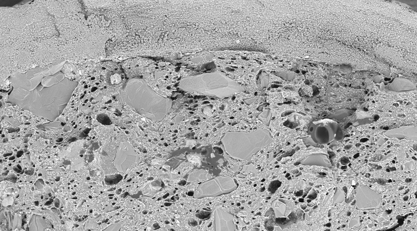
Using advanced SEM technology, we can visualize and document surface structures with incredible detail, highlighting features at the micro and nano-scale. This service is essential for researchers and industries that require precise imaging to evaluate material properties.
2. Detailed Analysis
Our team can determine the distribution and orientation of micro and nano-particles within a material. We also offer the ability to map the subsurface features, such as air voids or foreign particles, which are crucial for quality control and material integrity assessments.
3. Morphological Insights
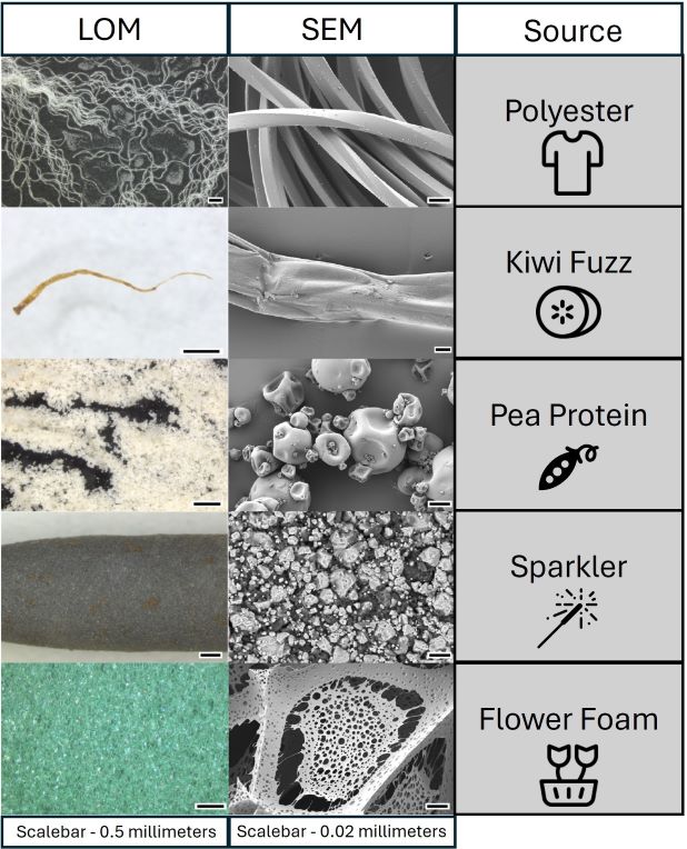
We provide detailed examinations of particle samples, focusing on their morphology and any tendencies for agglomeration. This analysis is vital for applications in pharmaceuticals, materials science, and industrial processing.
4. Elemental Mapping
With EDX technology, we map the elemental distribution across sample cross-sections or surfaces. This capability is invaluable for understanding the composition and distribution of elements within a sample, supporting materials development and failure analysis.
5. Identification Services
Our experts are skilled in identifying unknown materials, particles, or coatings by thoroughly analyzing their structure and elemental composition. This service is crucial for industries facing challenges with contaminants or needing verification of material specifications.
6. Precision Measurements
We measure the thickness of nano and micrometer-thick layers on surfaces, providing precise data that is critical for nanotechnology applications and advanced manufacturing processes.
How Can We Assist You?
Whether you are involved in research, development, or quality assurance, our SEM/EDX services offer the detailed insights required to understand and optimize your materials and processes.
Our laboratories undergo internal audits once a year. All of our analysis techniques are regularly checked against traceable reference materials.
The Danish Technological Institute is DANAK-accredited for examining unknown materials and identifying foreign objects. The investigations meet a quality standard that is typically approved by the FDA during company audits.
If you have any questions about our methods, please feel free to contact Kathrine Bjørneboe at 7220 3305 or kbj@teknologisk.dk.